This page was originally at wiki.seeedstudio.com.
Introduction
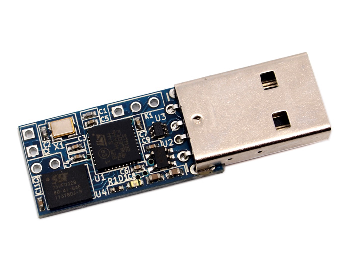
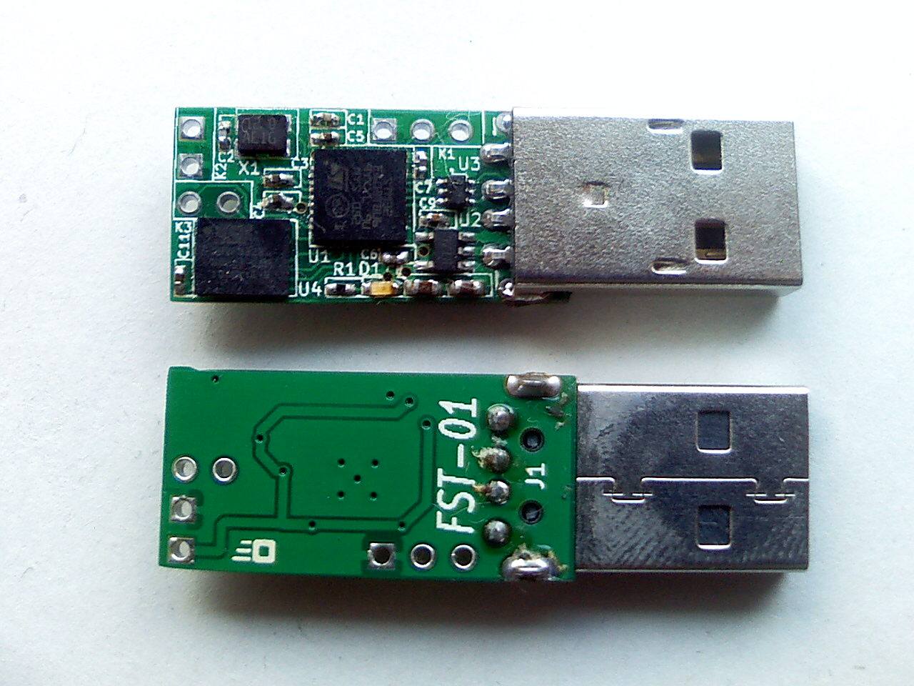
FST-01 is a tiny USB 32-bit computer. In fact, FST-01 is an abbreviation and its full name is "Flying Stone Tiny ZERO-ONE".
It is designed by Flying Stone Technology, a company in Maebashi, Gunma, Japan in 2011.
The concept is "Minimalist Design". It is by free (as in freedom) hardware design. The intended applications are Gnuk (The Cryptographic Token for GnuPG) and NeuG (True Random Number Generator based on ADC noise). Those applications are Free Software, too.
Flying Stone Technology is a second source manufacturer of "Gnuk", which is copyrighted by the Non-Profit organization, Free Software Initiative of Japan.
For those who want rich features, please consider Leaf Maple (Cortex M3) or Maple Mini, instead.
                    SWD port
                    (GND, SWD-CLK, SWD-IO)
Power port +---------------------+
       Vdd |[]           []()() -------+
       GND |[]                  |      |
           |()() I/O port       | USB  |
           |      (PA2, PA3)    |      |
           |                    -------+
           +---------------------+
Please see FST-01 support pages for your questions. You can ask to Gnuk Mailing Lists for Gnuk and NeuG.
Applications
As explained in the section above, we intend to run Gnuk on FST-01. It is copyrighted software distributed under GPLv3+ license.

Gnuk is an implementation of Cryptographic Token for GnuPG, and it runs on STM32F103. Source code is available at gniibe.org or git.debian.org.
For corresponding source code to the FST-01 at Seeed Studio, please visit: https://salsa.debian.org/gnuk-team/gnuk/gnuk/-/tree/release/1.0.1
For more information about Gnuk, please visit Official Gnuk Documentation.
Also, we intend to use FST-01 as NeuG standalone device.

NeuG is an implementation of True Random Number Generator based on quantization error of ADC.
Note that only an application can be installed on FST-01; FST-01 can be either of, Gnuk Token, or NeuG standalone device.
Development Environment
For Gnuk 1.0.1, we used GCC ARM Embedded 4.6-2012-q2: https://launchpad.net/gcc-arm-embedded/+milestone/4.6-2012-q2-update
Nowadays, we use: https://tracker.debian.org/pkg/gcc-arm-none-eabi
For the first lot of FST-01
In the product, it contains copyrighted software, Gnuk version 1.0.1, that is licensed under the GPLv3. A copy of that license is included in the source code. You may obtain the complete Corresponding Source code for a period of three years after the last shipment of the product, which will be no earlier than 2017-01-01, on the manufacturer website at https://git.gniibe.org/cgit/gnuk/gnuk.git/ and we put the tag "release/1.0.1" for the version of the product.
Note that Gnuk binary in the first lot of FST-01 was compiled with "-O3 -Os" option by GCC ARM Embedded 4.6-2012-q2.
Mailing list for Gnuk/NeuG
We have a mailing list for Gnuk/NeuG: https://lists.gnupg.org/mailman/listinfo/gnuk-users
As well as git.gniibe.org, the source code repositories are available at: https://salsa.debian.org/gnuk-team/gnuk
Writing flash ROM of MCU
We use SWD port to write flash ROM of MCU.
SWD was a kind of new in 2011, there had been not yet good hardware and software experiences.
Thus, we selected ST-Link/V2 for cheap SWD debugger and wrote our own tool stlinkv2.py in Python. The tool stlinkv2.py is distributed within Gnuk. See the article about FST-01 and SWD for the connection of ST-Link/V2 and FST-01.
Nowadays (as of 2016), OpenOCD 0.9.0 supports ST-Link/V2 and SWD very well. You can use that, too.
Products available at Seeed Bazaar (From the end of September 2012)
- FST-01 without enclosure: http://www.seeedstudio.com/depot/fst01-without-enclosure-p-1276.html
- FST-01 with heat shrink tube: http://www.seeedstudio.com/depot/fst01-with-heat-shrink-tube-p-1277.html
- FST-01 with case (P1A-120704U): http://www.seeedstudio.com/depot/fst01-with-white-enclosure-p-1279.html
Prices will be 35, 36, and 37 USD, respectively.
It is also available at Flying Stone Technology (飛石技術), person to person. See Buy FST-01! page at gniibe.org (in Japanese).
Description
FST-01 is minimum STM32F103 board, which is suitable to run computation-oriented applications like Gnuk.
- Dimensions: 1.62 x 0.52 inch (including USB plug)
- USB Bus Powered
- MCU: 32-bit ARM Cortex M3 at 72MHz (STM32F103TBU6), flash ROM: 128KB, RAM: 20KB
- SPI Flash Memory: 4MB
- SWD port, Two I/O pins
- Content of Flash ROM of MCU: As a side effect of the test plan, FST-01 comes with Gnuk version 1.0.1 installed on the flash ROM of MCU and it is protected. You need to disable the protection before writing the flash ROM.
Please visit this page (original wiki page) for detail.
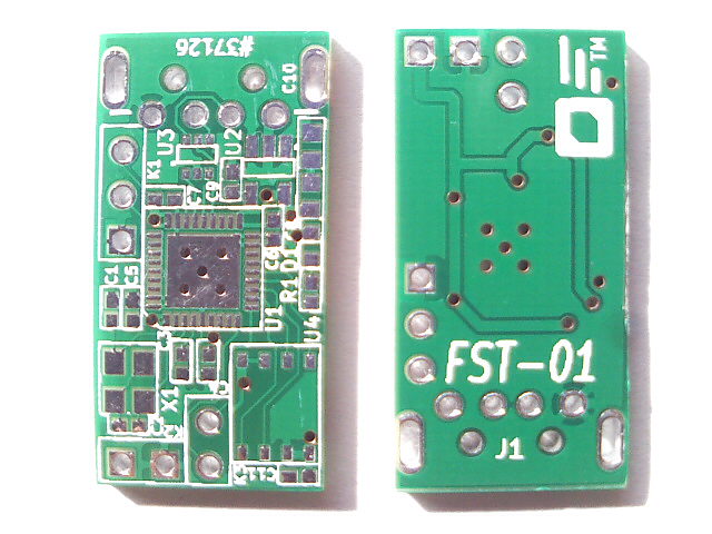
FST-01 without enclosure
This is a bare board for evaluation, development or those who want their own enclosures.
You can access SWD port and change the content of flash ROM.
FST-01 with heat shrink tube
The board is covered by transparent heat shrink tube. Thus, it is not possible to access SWD port.
This can be daily use as Gnuk Token.
FST-01 with case (P1A-120704U)
The board comes with the case. Note that it is users who put the board to the case.
This would be better if transparent tube doesn't match your taste or you want to change the content of flash ROM of MCU.
Although FST-01 PCB is designed following the recommendation of P1A-120704U specification, the case might be a bit larger and you will need a bit of glue to fit the board and the case. Otherwise, the board will be able to move a bit (< 1mm or so).
History
- 2011-08-06: Idea
- 2011-08-08: Initial commit to FST-01 Git repository
- 2011-08-23: Fusion PCB order for prototype PCB: #33163
- 2011-08-26: Wish for FST-01
- 2011-09-06: Fusion PCB order for prototype PCB: #34012
- 2011-09-13: Fusion PCB order for prototype PCB: #34217
- 2011-09-30: Fusion PCB order for prototype PCB: #35421
- 2011-10-27: Fusion PCB order for prototype PCB: #37126
- 2011-11-14: Version 1.0 of FST-01 PCB Design released
- 2012-07-10: Submitted to Propagete
- 2012-08-??: Placed the order for production
- 2012-09-27: Production finish for the first lot
- For the first lot, XTAL is changed to one with 20pF load capacitance. (Because of availability of the part.)
- For the first lot, content of flash ROM of MCU is Gnuk 1.0.1 and it's protected.
- 2012-10-08: Start selling at Seeed Bazaar
- 2015-04-01: Start selling at FSF Shop, with NeuG installed
Free (as in freedom) Board Design

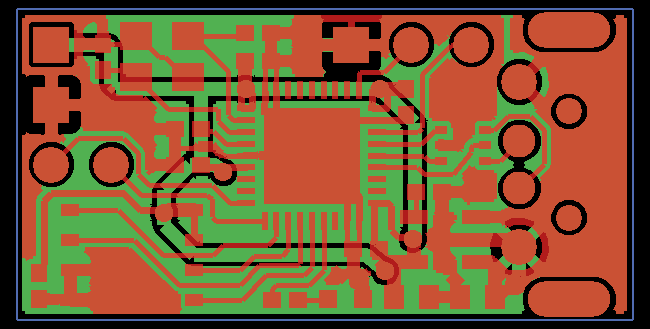
The board design is available as KiCAD format. Please visit FST-01 Git repository.
The schematic design is distributed under Creative Commons Attribution 3.0 Unported License (CC BY 3.0).
The PCB design is distributed under Creative Commons Attribution-ShareAlike 3.0 Unported License (CC BY-SA 3.0).
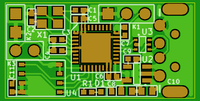
BOM of FST-01
| Part # | Name | Detail | Package | Manufacturer | Distributor | distributor reference |
|---|---|---|---|---|---|---|
| C1 | Capacitor | 27pF | C0402 | |||
| C2 | Capacitor | 27pF | C0402 | |||
| C3 | Capacitor | 0.1uF | C0402 | |||
| C4 | Capacitor | 0.1uF | C0402 | |||
| C5 | Capacitor | 0.1uF | C0402 | |||
| C6 | Capacitor | 0.1uF | C0402 | |||
| C7 | Capacitor | 0.1uF | C0402 | |||
| C8 | Capacitor | 4.7uF | C0603 | |||
| C9 | Capacitor | 0.01uF | C0402 | |||
| C10 | Capacitor | 4.7uF | C0603 | |||
| C11 | Capacitor | 0.1uF | C0402 | |||
| R1 | Resister | 510R | R0402 | |||
| D1 | LED | Blue | LED0603 | |||
| J1 | Connector | USB 2.0, 1002-015-01001 | USB Plug A Male | CNC Tech | Digikey | 1175-1020-ND |
| U1 | MCU | STM32F103TBU6 | QFN36 | ST Microelectronics | AVNET | STM32F103TBU6 |
| U2 | LDO V-Regulator | CAT6217-330TDGT3 +3.3V | TSOT23-5 | ON Semiconductor | Mouser | 698-CAT6217330TD-G |
| U3 | USB Terminator | NUF2221W1 | SOT363 | ON Semiconductor | Digikey | NUF2221W1T2GOSTR-ND |
| U4 | SPI Flash Memory | SST25VF032B-80-4I-QAE-T | WSON8 | Silicon Storage Technology | Digikey | SST25VF032B-80-4I-QAE-T-ND |
| X1 | Crystal | ABM8G-12.000MHZ-18-D2Y-T | 3.2mmx2.5mm | Abracon Corporation | Digikey | 535-10261-2-ND |
| Enclosure | P1A-120704U White | 1.2x.71x.40 '' | New Age Enclosures |
Components of FST-01
- STM32F103TB
- SPI Flash memory (32Mbit)
- USB Terminator
- LDO Regulator (3.3V)
- 12MHz XTAL CL=18pF
- LED
- SWD Port of GND/SWDIO/SWDCLK
- Extension port of VDD/GND/Port0/Port1
- USB plug A
STM32F103TB
MCU is Cortex-M3 based ARM by STMicroelectronics. It runs at 72MHz, it has 128KB flash ROM and 20KB RAM.
SPI Flash memory
Secret data should be on MCU's flash, but non confidential data (such as backup of public keyring) can be on SPI flash memory.
We use SST25VF032B (32Mbit = 4MB).
USB Terminator
We use NUF2221W1 USB Upstream Terminator.
This is because it has the feature of electrostatic discharge protection. It is also better for smaller footprint than two capacitors and two resistors.
LDO Regulator
We use CAT6217-330 for 3.3V Regulator (from 5V). Currency of 150mA is enough.
XTAL 12MHz CL=18pF
We use 12MHz XTAL CL=18pF.
This is because we can find smaller footprint XTAL for 12MHz (than 8MHz).
LED
We use a LED to show status.
SWD port
SWD port is to install firmware to MCU's flash ROM.
Extension port of VDD/GND/Port0/Port1
We decided to have two I/O pins. (One I/O pin is not enough even for minimalist.)
With two I/O pins, it can be:
- TX and RX of serial communication
- Drive and input of touch sensor
- Controlling other MCU's SWD port
USB plug A
FST-01 usage is just connect it to USB port, like USB thumb drive.
Possible Changes to the circuit and parts
LDO Regulator
MCP1700T-330 would be alternative (electrical characteristic seems worse, but for the case of more current). In this case, we need to change circuit a bit.
XTAL
It is possible to just replace XTAL with 12MHz XTAL CL=20pF. This change is within the margin of the design.
It would be better to also replace C1 and C2 to 33pF together in that case, if you will do that from the beginning.
Shield GND to Signal GND
FST-01 is intended to be inserted to USB port directly. If the usage is not direct but connected by extension cable, it is better to connect Shield GND and Signal GND by resister (and capacitor if you like).
Reference: http://electronics.stackexchange.com/questions/4515/how-to-connect-usb-connector-shield
USB_EN
USB_EN is not needed, but pin 5 of NUF2221W1 can be connected to 3.3V (Vdd) directly.
In many designs of boards with STM32F103, we see something like that, but because it is possible to control USB D+ to be 0V by software, USB_EN is not needed.
No SPI flash memory by default
The size is somewhat too small to be useful, so, it could be a special users' option and no chip would be OK by default.

Engineering Prototype of FST-01
Thanks to Fusion PCB service, we made PCB of FST-01 Engineering Prototype.
PCB Assembly was done by gniibe manually. See the DIY article for detail.
Test plan outline
- Check MCU ID
- Write to flash ROM of MCU
- Check LED blinking
- Check SPI Flash ROM access
- Run an application which uses USB and see if it works (Hub assigning address)
- On power up (or reset), LED emits light.
- FST-01 application waits for USB address assignment by USB Hub. (It takes a few seconds for Hub to detect and to assign address to the device.)
- After USB address assignment, FST-01 application goes enter the loop
- waiting 5 seconds
- blink LED (emits lights for 25ms,off 200ms).