Use of XOR accumulator
I draw another schematics, the main part is like following.
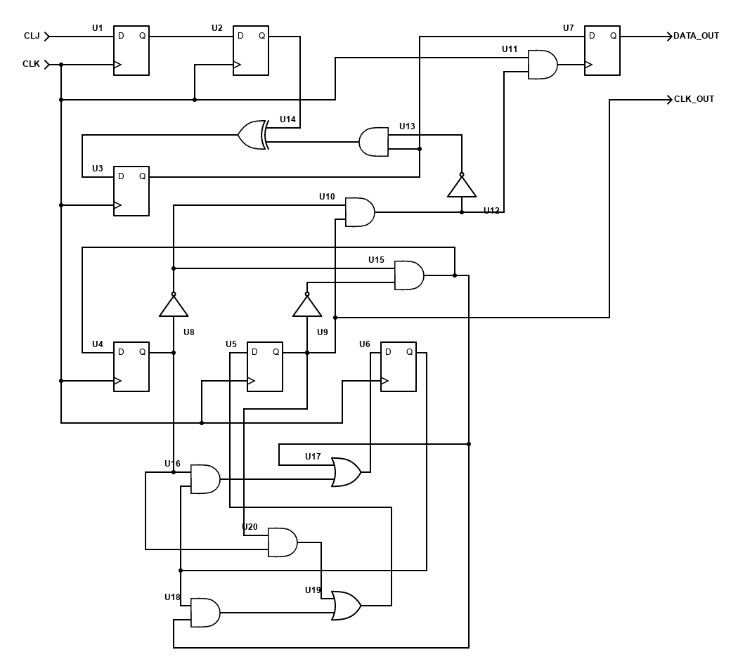
Instead of a shift register and a set of xor gates, it only uses an accumulator and a single xor gate.
The shift register was used because I had an idea of changing the shift register into linear feedback shift register (LFSR). When it's LFSR, it has a state of bits which makes guessing a bit difficult (that is, adding obfuscation to the machinery).
But adding obfuscation in earlier stage is not good to evaluate the mechanism, so, I decided make it simpler. Obfuscation can/should be done in later stage.
Second entry: 192-567-256 for GW1NR-9C
The second entry is: 256/567 for Tang Nano 9K. That is,
- Target FPGA is GW1NR-9C
- CLJ = 425.25MHz
- CLK = 192MHz
- Generation speed: 0.75Mbps
- Base clock is 192MHz (so that we can build USB function with 48MHz).
- Using 27MHz clock input of Tang Nano 9K
If we can use our own external clock, with 128MHz clock input, we can use 288-256-225.
Thanks to Project Apicula, the release 0.7 allows us to use its PLLs.
Comparison: GW1NR-9C and iCE40 HX8K
With GW1NR-9C, its random number generation speed is smaller, unfortunately (0.75Mbps). Apparently, GW1NR-9C has a better (less jitter) PLL than iCE40 HX8K. It's good for the intended normal use of PLL, but for building RNG, somehow, noisy PLL is rather useful.
Besides, to build a PLL-based RNG, support of larger multiplication factor is important. In this regard, iCE40 is better too (which allows multiplying by 127. GW1NR-9C has multiplication factor up to 64).