I start a project, named Gomti. It's a collection of configurations and implementations to build a PLL-based true random number generater (TRNG). The central part of Gomti is actually, curated rational numbers to build PLL RNG.
The name
The name "gomti" is an acronym to remember the first part of this conversation:
Gen1: One man's trash is...
Gen2: ... another man's treasure.
Purpose and why Gomti
More entropy is needed, but there is not good TRNG technology, which people can examine, test, evaluate, use it freely (as in freedom).
I implemented NeuG, for devices with MCU as free software, where no built-in TRNG is avaliable in the MCU. However, it has no mathmatical stochastic model, nor physical model. While I say that NeuG generates random numbers people cannot guess, it is hard to prove none can guess.
I sought around TRNG technology which we can use. Conditions are:
- Easier to implement (cost-wise, technology-wise)
- Patent free
- Better reproducibility
- We can build a device with common parts
- We can build a device using free tool (as in freedom)
In 2022, I concluded that PLL-based TRNG with FPGA/ASIC fullfills these conditions. That's because free tool for FPGA is now available.
Structure of PLL-based TRNG and Its Mathmatical Model
It uses two clocks with rationally related frequencies to generate random numbers.
+----+  CLJ  +-----------+
|Gen1|------>|           |        +-----------------+
+----+       |           |        |                 | Random numbers
             |  Sampler  |------->| Post-processing |-------------->
+----+  CLK  |           |        |                 |
|Gen2|------>|           |        +-----------------+
+----+       +-----------+
First entry: 240-127-120 for iCE40 HX8K
The first one is: 120/127 for iCE40 HX8K. That is,
- Target FPGA is iCE40 HX8K.
- CLJ = 254MHz
- CLK = 240MHz
- Generation speed: 2Mbps
- Base clock is 240MHz (so that we can build USB function with 48MHz).
If I draw a schematics for this, the main part is like following.
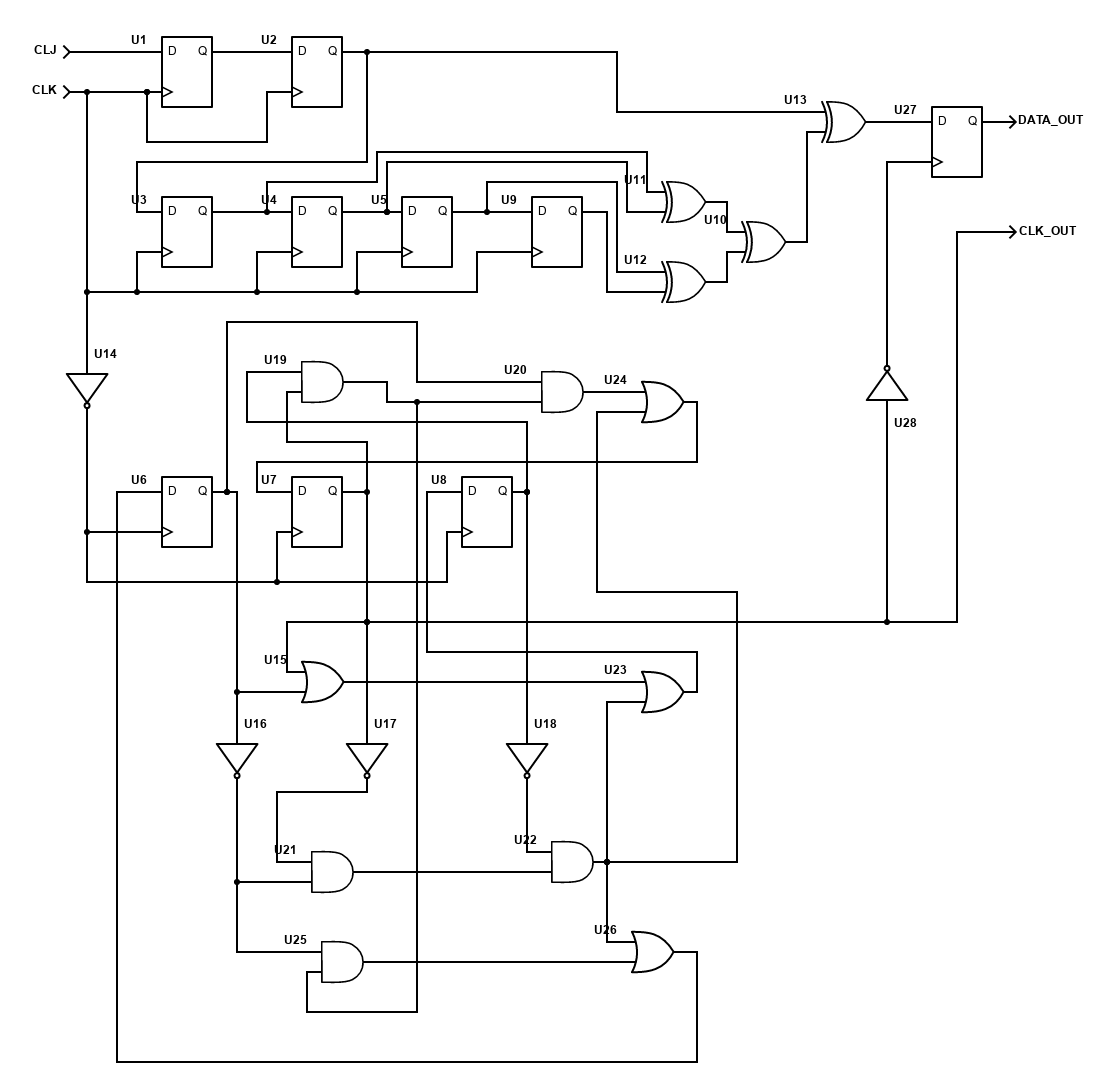
That is, a synchronizer, a shift register, a counter and xor-ed output FF.
This is for existing boards (iCE40 HX8K Breakout board and Alchitry Cu board).
If we can use our own external clock, with 64MHz clock input, we can use 240-116-105.
References
| [1] | Viktor Fischer & Miloš Drutarovský
|
| [2] | Florent Bernard, Viktor Fischer and Boyan Valtchanov
|
| [3] | Miloš Drutarovský and Martin Simka and Viktor Fischer and Frederic Celle
|